- 您现在的位置:买卖IC网 > Sheet目录2004 > LTC1662IN8#PBF (Linear Technology)IC D/A CONV 10BIT MICRPWR 8-DIP
LTC1662
9
1662fa
operation
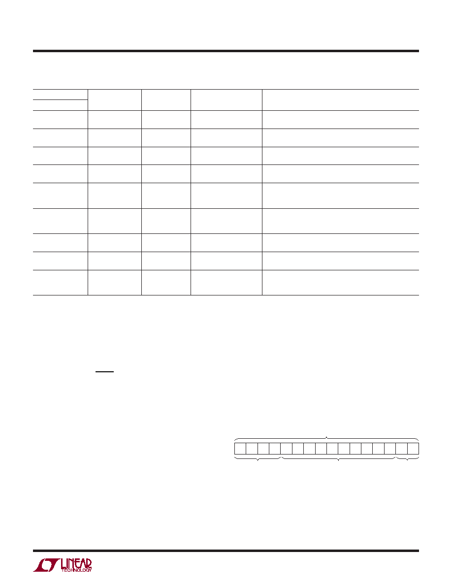
Table 1. DAC Control Functions
CONTROL
INPUT REGISTER
STATUS
DAC REGISTER
STATUS
POWER-DOWN STATUS
(SLEEP/WAKE)
COMMENTS
A3 A2 A1 A0
0
No Change
No Update
No Change
No Operation. Power-Down Status Unchanged
(Part Stays In Wake or Sleep Mode)
0
1
Load DAC A
No Update
No Change
Load Input Register A with Data. DAC Outputs Unchanged.
Power-Down Status Unchanged
0
1
0
Load DAC B
No Update
No Change
Load Input Register B with Data. DAC Outputs Unchanged.
Power-Down Status Unchanged
1
0
No Change
Update Outputs
Wake
Load Both DAC Regs with Existing Contents of Input Regs.
Outputs Update. Part Wakes Up
1
0
1
Load DAC A
Update Outputs
Wake
Load Input Reg A. Load DAC Regs with New Contents of
Input Reg A and Existing Contents of Reg B. Outputs Update.
Part Wakes Up
1
0
1
0
Load DAC B
Update Outputs
Wake
Load Input Reg B. Load DAC Regs with Existing Contents of
Input Reg A and New Contents of Reg B. Outputs Update.
Part Wakes Up
1
0
1
No Change
No Update
Wake
Part Wakes Up. Input and DAC Regs Unchanged.
DAC Outputs Reflect Existing Contents of DAC Regs
1
0
No Change
No Update
Sleep
Part Goes to Sleep. Input and DAC Regs Unchanged.
DAC Outputs Set to High Impedance State
1
Load DACs A, B
with Same
10-Bit Code
Update Outputs
Wake
Load Both Input Regs. Load Both DAC Regs with New
Contents of Input Regs. Outputs Update. Part Wakes Up
Note: All control codes other than those shown are undefined and not subject to test.
Transfer Function
The transfer function for the LTC1662 is:
VOUT(IDEAL) =
k
1024
VREF
where k is the decimal equivalent of the binary DAC input
code D9-D0 and VREF is the voltage at REF (Pin 4).
Power-On Reset
The LTC1662 actively clears the outputs to zero-scale
when power is first applied, making system initialization
consistent and repeatable.
Power Supply Sequencing
The voltage at REF (Pin 4) should be kept within the range
–0.3V ≤ VREF ≤ VCC + 0.3V (see the Absolute Maximum
Ratings). Particular care should be taken during power
supplyturn-onandturn-offsequences,whenthevoltageat
VCC (Pin 6) is in transition. If it is not possible to sequence
the supplies, clamp the voltage at REF by connecting a
SchottkydiodebetweenPin4(anode)andPin6(cathode).
Serial Interface
See Table 2. The 16-bit input word consists of the 4-bit
controlcode,the10-bitinputcodeandtwodon’t-carebits.
Table 2. LTC1662 Input Word
A3 A2 A1
Control Code
A0 D9 D8 D7 D6 D5 D4 D3 D2 D1
X1 X0
D0
Input Code
Input Word
Don’t
Care
Aftertheinputwordisloadedintotheregister(seeFigure1),
it is internally converted from serial to parallel format. The
parallel 10-bit-wide input code data path is then buffered
by two latch registers.
发布紧急采购,3分钟左右您将得到回复。
相关PDF资料
LTC1663-1CS5#TRM
IC DAC 10BIT R-R TSOT23-5
LTC1664IN
IC DAC 10BIT QUAD MICRPWR 16DIP
LTC1667CG#PBF
IC D/A CONV 14BIT 50MSPS 28-SSOP
LTC1686IS8#TRPBF
IC TXRX RS485 PREC DELAY 8-SOIC
LTC1688IS
IC DVR 100MBPS RS485 QUAD 16SOIC
LTC1690IS8#TRPBF
IC RCVR/DVR PAIR LOW PWR 8-SOIC
LTC1740IG#TRPBF
IC ADC 14BIT 6MSPS 36SSOP
LTC1741IFW#PBF
IC ADC 12BIT 65MSPS 48-TSSOP
相关代理商/技术参数
LTC1663-1CS5
制造商:Linear Technology 功能描述:DAC 1-CH 10-bit 5-Pin TSOT-23
LTC1663-1CS5#PBF
制造商:Linear Technology 功能描述:DAC 1-CH 10-bit 5-Pin TSOT-23
LTC1663-1CS5#TR
功能描述:IC DAC 10BIT R-R TSOT23-5 RoHS:否 类别:集成电路 (IC) >> 数据采集 - 数模转换器 系列:- 产品培训模块:Data Converter Fundamentals
DAC Architectures 设计资源:Unipolar, Precision DC Digital-to-Analog Conversion using AD5450/1/2/3 8-14-Bit DACs (CN0052)
Precision, Bipolar, Configuration for AD5450/1/2/3 8-14bit Multiplying DACs (CN0053)
AC Signal Processing Using AD5450/1/2/3 Current Output DACs (CN0054)
Programmable Gain Element Using AD5450/1/2/3 Current Output DAC Family (CN0055)
Single Supply Low Noise LED Current Source Driver Using a Current Output DAC in the Reverse Mode (CN0139) 标准包装:10,000 系列:- 设置时间:- 位数:12 数据接口:DSP,MICROWIRE?,QSPI?,串行,SPI? 转换器数目:1 电压电源:单电源 功率耗散(最大):- 工作温度:-40°C ~ 125°C 安装类型:表面贴装 封装/外壳:SOT-23-8 薄型,TSOT-23-8 供应商设备封装:TSOT-23-8 包装:带卷 (TR) 输出数目和类型:1 电流,单极;1 电流,双极 采样率(每秒):2.7M
LTC1663-1CS5#TRM
功能描述:IC DAC 10BIT R-R TSOT23-5 RoHS:否 类别:集成电路 (IC) >> 数据采集 - 数模转换器 系列:- 产品培训模块:Lead (SnPb) Finish for COTS
Obsolescence Mitigation Program 标准包装:1,000 系列:- 设置时间:1µs 位数:8 数据接口:串行 转换器数目:8 电压电源:双 ± 功率耗散(最大):941mW 工作温度:0°C ~ 70°C 安装类型:表面贴装 封装/外壳:24-SOIC(0.295",7.50mm 宽) 供应商设备封装:24-SOIC W 包装:带卷 (TR) 输出数目和类型:8 电压,单极 采样率(每秒):*
LTC1663-1CS5#TRMPBF
功能描述:IC DAC 10BIT R-R TSOT23-5 RoHS:是 类别:集成电路 (IC) >> 数据采集 - 数模转换器 系列:- 产品培训模块:Data Converter Fundamentals
DAC Architectures 标准包装:3,000 系列:nanoDAC™ 设置时间:80µs 位数:18 数据接口:DSP,MICROWIRE?,QSPI?,串行,SPI? 转换器数目:1 电压电源:单电源 功率耗散(最大):- 工作温度:-40°C ~ 105°C 安装类型:表面贴装 封装/外壳:SOT-23-8 供应商设备封装:SOT-23-8 包装:带卷 (TR) 输出数目和类型:1 电压,单极 采样率(每秒):- 产品目录页面:784 (CN2011-ZH PDF) 配用:EVAL-AD5680EBZ-ND - BOARD EVAL FOR AD5680 其它名称:AD5680BRJZ-2REEL7TR
LTC1663-1CS5#TRPBF
功能描述:IC DAC 10BIT R-R TSOT23-5 RoHS:是 类别:集成电路 (IC) >> 数据采集 - 数模转换器 系列:- 产品培训模块:Data Converter Fundamentals
DAC Architectures 设计资源:Unipolar, Precision DC Digital-to-Analog Conversion using AD5450/1/2/3 8-14-Bit DACs (CN0052)
Precision, Bipolar, Configuration for AD5450/1/2/3 8-14bit Multiplying DACs (CN0053)
AC Signal Processing Using AD5450/1/2/3 Current Output DACs (CN0054)
Programmable Gain Element Using AD5450/1/2/3 Current Output DAC Family (CN0055)
Single Supply Low Noise LED Current Source Driver Using a Current Output DAC in the Reverse Mode (CN0139) 标准包装:10,000 系列:- 设置时间:- 位数:12 数据接口:DSP,MICROWIRE?,QSPI?,串行,SPI? 转换器数目:1 电压电源:单电源 功率耗散(最大):- 工作温度:-40°C ~ 125°C 安装类型:表面贴装 封装/外壳:SOT-23-8 薄型,TSOT-23-8 供应商设备封装:TSOT-23-8 包装:带卷 (TR) 输出数目和类型:1 电流,单极;1 电流,双极 采样率(每秒):2.7M
LTC1663-2CS5#TR
功能描述:IC DAC 10BIT R-R TSOT23-5 RoHS:否 类别:集成电路 (IC) >> 数据采集 - 数模转换器 系列:- 产品培训模块:Data Converter Fundamentals
DAC Architectures 设计资源:Unipolar, Precision DC Digital-to-Analog Conversion using AD5450/1/2/3 8-14-Bit DACs (CN0052)
Precision, Bipolar, Configuration for AD5450/1/2/3 8-14bit Multiplying DACs (CN0053)
AC Signal Processing Using AD5450/1/2/3 Current Output DACs (CN0054)
Programmable Gain Element Using AD5450/1/2/3 Current Output DAC Family (CN0055)
Single Supply Low Noise LED Current Source Driver Using a Current Output DAC in the Reverse Mode (CN0139) 标准包装:10,000 系列:- 设置时间:- 位数:12 数据接口:DSP,MICROWIRE?,QSPI?,串行,SPI? 转换器数目:1 电压电源:单电源 功率耗散(最大):- 工作温度:-40°C ~ 125°C 安装类型:表面贴装 封装/外壳:SOT-23-8 薄型,TSOT-23-8 供应商设备封装:TSOT-23-8 包装:带卷 (TR) 输出数目和类型:1 电流,单极;1 电流,双极 采样率(每秒):2.7M
LTC1663-2CS5#TRM
功能描述:IC DAC 10BIT R-R TSOT23-5 RoHS:否 类别:集成电路 (IC) >> 数据采集 - 数模转换器 系列:- 产品培训模块:Data Converter Fundamentals
DAC Architectures 设计资源:Unipolar, Precision DC Digital-to-Analog Conversion using AD5450/1/2/3 8-14-Bit DACs (CN0052)
Precision, Bipolar, Configuration for AD5450/1/2/3 8-14bit Multiplying DACs (CN0053)
AC Signal Processing Using AD5450/1/2/3 Current Output DACs (CN0054)
Programmable Gain Element Using AD5450/1/2/3 Current Output DAC Family (CN0055)
Single Supply Low Noise LED Current Source Driver Using a Current Output DAC in the Reverse Mode (CN0139) 标准包装:10,000 系列:- 设置时间:- 位数:12 数据接口:DSP,MICROWIRE?,QSPI?,串行,SPI? 转换器数目:1 电压电源:单电源 功率耗散(最大):- 工作温度:-40°C ~ 125°C 安装类型:表面贴装 封装/外壳:SOT-23-8 薄型,TSOT-23-8 供应商设备封装:TSOT-23-8 包装:带卷 (TR) 输出数目和类型:1 电流,单极;1 电流,双极 采样率(每秒):2.7M